- 您现在的位置:买卖IC网 > Sheet目录408 > DMP2104LP-7 (Diodes Inc)MOSFET P-CH 20V 1.5A 3-DFN
�� ���
���
���DMP2104LP�
�P-CHANNEL� ENHANCEMENT� MODE� FIELD� EFFECT� TRANSISTOR�
�Features�
�Mechanical� Data�
�?�
�?�
�?�
�?�
�?�
�?�
�?�
�?�
�?�
�?�
�P-Channel� MOSFET�
�Very� Low� On-Resistance�
�Very� Low� Gate� Threshold� Voltage�
�Low� Input� Capacitance�
�Fast� Switching� Speed�
�Low� Input/Output� Leakage�
�Ultra-Small� Surface� Mount� Package�
�Lead� Free� By� Design/RoHS� Compliant� (Note� 2)�
�"Green"� Device� (Note� 3)�
�Qualified� to� AEC-Q101� Standards� for� High� Reliability�
�?�
�?�
�?�
�?�
�?�
�?�
�?�
�?�
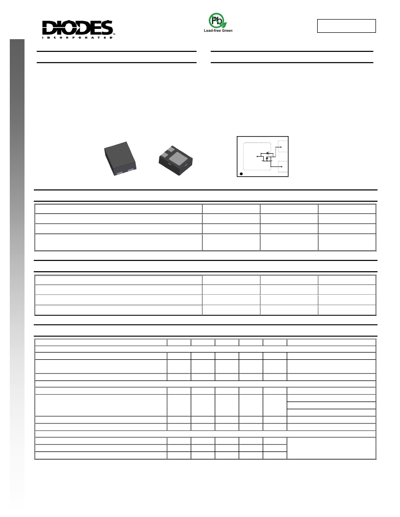
�Case:� DFN1411-3�
�Case� Material:� Molded� Plastic,� “Green”� Molding�
�Compound.� UL� Flammability� Classification� Rating� 94V-0�
�Moisture� Sensitivity:� Level� 1� per� J-STD-020C�
�Terminal� Connections:� See� Diagram�
�Terminals:� Finish� -� NiPdAu� over� Copper� lead� frame.�
�Solderable� per� MIL-STD-202,� Method� 208�
�Marking� Information:� See� Page� 3�
�Ordering� Information:� See� Page� 3�
�Weight:� 0.003� grams� (approximate)�
�DFN1411-3�
�S�
�D�
�G�
�TOP� VIEW�
�BOTTOM� VIEW�
�TOP� VIEW�
�Internal� Schematic�
�Maximum� Ratings�
�@T� A� =� 25°C� unless� otherwise� specified�
�Drain-Source� Voltage�
�Gate-Source� Voltage�
�Characteristic�
�Symbol�
�V� DSS�
�V� GSS�
�Value�
�-20�
�±12�
�Units�
�V�
�V�
�Continuous� Drain� Current� (Note� 1)�
�T� A� =� 25°C�
�T� A� =� 70°C�
�I� D�
�-1.5�
�-1.2�
�A�
�Thermal� Characteristics�
�@T� A� =� 25°C� unless� otherwise� specified�
�Characteristic�
�Power� Dissipation� (Note� 1)�
�Thermal� Resistance,� Junction� to� Ambient� (Note� 1)�
�Operating� and� Storage� Temperature� Range�
�Symbol�
�P� D�
�R� θ� JA�
�T� j,� T� STG�
�Value�
�500�
�250�
�-55� to� +150�
�Units�
�mW�
�°C/W�
�°C�
�Electrical� Characteristics�
�@T� A� =� 25°C� unless� otherwise� specified�
�Characteristic�
�Symbol�
�Min�
�Typ�
�Max�
�Unit�
�Test� Condition�
�OFF� CHARACTERISTICS� (Note� 4)�
�Drain-Source� Breakdown� Voltage�
�BV� DSS�
�-20�
�?�
�?�
�V�
�V� GS� =� 0V,� I� D� =� -250� μ� A�
�Zero� Gate� Voltage� Drain� Current�
�Gate-Source� Leakage�
�T� J� =� 25� °� C�
�T� J� =� 125� °� C�
�I� DSS�
�I� GSS�
�?�
�?�
�?�
�?�
�-1.0�
�-5.0�
�±� 100�
�μ� A�
�nA�
�V� DS� =� -20V,� V� GS� =� 0V�
�V� GS� =� ±� 12V,� V� DS� =� 0V�
�ON� CHARACTERISTICS� (Note� 4)�
�Gate� Threshold� Voltage�
�Static� Drain-Source� On-Resistance�
�Forward� Transconductance�
�Diode� Forward� Voltage� (Note� 4)�
�V� GS(th)�
�R� DS� (ON)�
�g� FS�
�V� SD�
�-0.45�
�?�
�?�
�?�
�?�
�92�
�134�
�180�
�3.1�
�?�
�-1.0�
�150�
�200�
�240�
�?�
�-0.9�
�V�
�m� Ω�
�S�
�V�
�V� DS� =� V� GS� ,� I� D� =� -250� μ� A�
�V� GS� =� -4.5V,� I� D� =� -950mA�
�V� GS� =� -2.5V,� I� D� =� -670mA�
�V� GS� =� -1.8V,� I� D� =� -200mA�
�V� DS� =� -10V,� I� D� =� -810mA�
�V� GS� =� 0V,� I� S� =� -360mA�
�DYNAMIC� CHARACTERISTICS�
�Input� Capacitance�
�Output� Capacitance�
�Reverse� Transfer� Capacitance�
�C� iss�
�C� oss�
�C� rss�
�?�
�?�
�?�
�320�
�80�
�60�
�?�
�?�
�?�
�pF�
�pF�
�pF�
�V� DS� =� -16V,� V� GS� =� 0V�
�f� =� 1.0MHz�
�Notes:�
�1.�
�2.�
�3.�
�4.�
�Device� mounted� on� FR-4� PCB� with� 1� inch� square� pads.�
�No� purposefully� added� lead.�
�Diodes� Inc.’s� “Green”� policy� can� be� found� on� our� website� at� http://www.diodes.com/products/lead_free/index.php.�
�Short� duration� pulse� test� used� to� minimize� self-heating� effect.�
�DMP2104LP�
�Document� number:� DS31091� Rev.� 6� -� 2�
�1� of� 4�
�www.diodes.com�
�November� 2007�
�?� Diodes� Incorporated�
�发布紧急采购,3分钟左右您将得到回复。
相关PDF资料
DMP2104V-7
MOSFET P-CH 20V 860MA SOT-563
DMP2123L-7
MOSFET P-CH 20V 3A SOT23-3
DMP2130L-7
MOSFET P-CH 20V 3A SOT23-3
DMP2130LDM-7
MOSFET P-CH 20V 3.4A SOT-26
DMP2160U-7
MOSFET P-CH 20V 3.2A SOT-23
DMP2160UW-7
MOSFET P-CH 20V 1.5A SOT-323
DMP21D0UFB4-7B
MOSF P CH 20V 770MA DFN1006H4-3
DMP21D0UFD-7
MOS P CH 20V 1.14A X1-DFN1212-3
相关代理商/技术参数
DMP2104V
制造商:DIODES 制造商全称:Diodes Incorporated 功能描述:P-CHANNEL ENHANCEMENT MODE FIELD EFFECT TRANSISTOR
DMP2104V_0711
制造商:DIODES 制造商全称:Diodes Incorporated 功能描述:P-CHANNEL ENHANCEMENT MODE FIELD EFFECT TRANSISTOR
DMP2104V-7
功能描述:MOSFET -20V -860mA RoHS:否 制造商:STMicroelectronics 晶体管极性:N-Channel 汲极/源极击穿电压:650 V 闸/源击穿电压:25 V 漏极连续电流:130 A 电阻汲极/源极 RDS(导通):0.014 Ohms 配置:Single 最大工作温度: 安装风格:Through Hole 封装 / 箱体:Max247 封装:Tube
DMP2104V-7-F
制造商:DIODES 功能描述:P-CHANNEL ENHANCEMENT MODE FIELD EFFECT TRANSISTOR
DMP210DUDJ
制造商:DIODES 制造商全称:Diodes Incorporated 功能描述:DUAL P-CHANNEL ENHANCEMENT MODE MOSFET
DMP210DUDJ-7
功能描述:MOSFET N-Ch Dual MOSFET 20V VDSS 8V VGSS RoHS:否 制造商:STMicroelectronics 晶体管极性:N-Channel 汲极/源极击穿电压:650 V 闸/源击穿电压:25 V 漏极连续电流:130 A 电阻汲极/源极 RDS(导通):0.014 Ohms 配置:Single 最大工作温度: 安装风格:Through Hole 封装 / 箱体:Max247 封装:Tube
DMP210DUFB4-7
制造商:DIODES 功能描述:P-CHANNEL ENHANCEMENT MODE FIELD EFFECT TRANSISTOR
DMP210DUFB4-7B
制造商:DIODES 功能描述:P-CHANNEL ENHANCEMENT MODE MOSFET